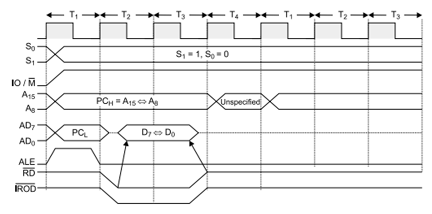
Draw And Explain The Timing Diagram For Opcode Fetch Operation. The output device and terminates the writing operation. Ü the time taken by the processor to execute the opcode fetch cycle is 4t.
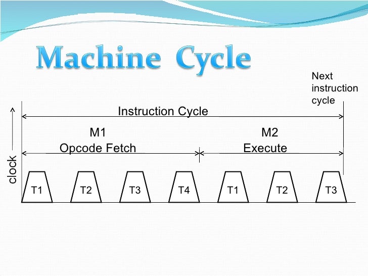
Usually, it consists of four t states. The timing diagram of inr m instruction is shown below: For the opcode fetch the io/m (low active) = 0, s1 = 1 and s0 = 1. First we look into its machine code 1. It require 3 m/c cycles 10 t states opcode fetch(4t) memory read(3t) i/o read(3t) collected by c.gokul ap/eee,vcet 19.
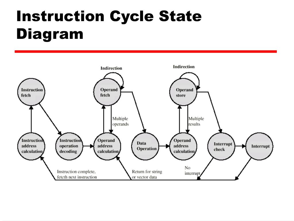
Opcode fetch machine cycle of 8085 :
When processor is ready to initiate the bus cycle, it applies a pulse to ale during t1. • read the content of port c0h and send it to the accumulator. • let the content of port is 5eh. The following points explain the various operations that take place and the signals that are changed during the execution of opcode fetch machine cycle: 35) draw and explain the timing diagram for opcode fetch operation 36) discuss various types of addressing modes of 8085. The timing diagram of inr m instruction is shown below: Redraw the diagram to show how many time units are now needed for four instructions. The machine cycle is exactly same to opcode fetch except: Once we understand this, it is very easy to draw timing diagram. Example fetch a byte 41h stored at memory location 2105h. For fetching a byte, the microprocessor must find out the memory location where it is stored. Provides signal for multiplexed address and data bus. The timing diagram of mov instruction is shown below:
• read the content of port c0h and send it to the accumulator. Figure 9.14 shows the timing diagram and data follow for io write machine cycle. Den = high and dt/r = 0 for input or dt/r = 1 for output. For fetching a byte, the microprocessor must find out the memory location where it is stored. Redraw the diagram to show how many time units are now needed for four instructions.
With help of timing diagram, we can easily calculate the execution time of instruction and as well as program.
During t1 state, microprocessor uses io/m (bar), s0, s1 signals are used to instruct microprocessor to fetch opcode. The opcodes are stored in memory. Example fetch a byte 41h stored at memory location 2105h. The time taken by the processor to execute the opcode fetch cycle is 4t. The output device and terminates the writing operation. First we look into its machine code 1. The machine cycle is exactly same to opcode fetch except: To indicate that the mpu is in fetch mode operation. So, the processor executes the opcode fetch machine cycle to fetch the opcode from memory. Define (a) instruction cycle, (b) machine cycle, (c) clock cycle.4. The timing diagram of mov instruction is shown below: Timing diagram of opcode fetch. Timing diagram for in c0h • fetching the opcode dbh from the memory 4125h.
Consider the timing diagram of figures 12.10. Op code fetch (4 clock standard fetch) without doing anything to stack pointer. Hence, every instruction starts with. Redraw the diagram to show how many time units are now needed for four instructions. Following is the timing diagram of the instruction lxi d, 56feh.
It is the first step in the execution of any instruction.
Higher bit of address where opcode is stored, i.e., 20. Figure 9.14 shows the timing diagram and data follow for io write machine cycle. With help of timing diagram, we can easily calculate the execution time of instruction and as well as program. First we look into its machine code 1. Once we understand this, it is very easy to draw timing diagram. The opcode fetch machine cycle (ofmc) involves the fetching of the opcode of the instruction to be executed and the decoding process of that opcode. Op code fetch (4 clock standard fetch) without doing anything to stack pointer. The memory read cycle is executed by the processor to read a data byte from memory. Lower bit of address where opcode is stored, i.e., 00 20: 8085 timing diagram for opcode fetch cycle for mov c, a. Memory read machine cycle of 8085: Ü the time taken by the processor to execute the opcode fetch cycle is 4t. Figure 12.10 timing diagram for instruction pipeline.